Switch content of the page by the Role togglethe content would be changed according to the role
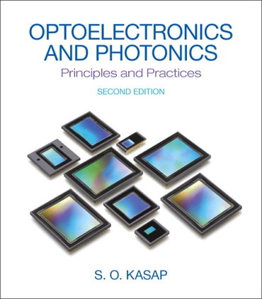
Optoelectronics & Photonics: Principles & Practices, 2nd edition
Published by Pearson (November 5, 2012) © 2013
- Safa O. Kasap University of Saskatchewan
$64.99
Instant access
Access details
- Instant access once purchased
- Fulfilled by VitalSource
- 180-day rental
Features
- Add notes and highlights
- Search by keyword or page
$202.66
Price Reduced From: $253.32
Details
- A print text
This product is expected to ship within 3-6 business days for US and 5-10 business days for Canadian customers.
For one-semester, undergraduate-level courses in Optoelectronics and Photonics, in the departments of electrical engineering, engineering physics, and materials science and engineering.
This text takes a fresh look at the enormous developments in electo-optic devices and associated materials.
Chapter 1 Wave Nature of Light 3
1.1 Light Waves in a Homogeneous Medium 3
A. Plane Electromagnetic Wave 3
B. Maxwell’s Wave Equation and Diverging Waves 6
Example 1.1.1 A diverging laser beam 10
1.2 Refractive Index and Dispersion 10
Example 1.2.1 Sellmeier equation and diamond 13
Example 1.2.2 Cauchy equation and diamond 14
1.3 Group Velocity and Group Index 14
Example 1.3.1 Group velocity 17
Example 1.3.2 Group velocity and index 17
Example 1.3.3 Group and phase velocities 18
1.4 Magnetic Field, Irradiance, and Poynting Vector 18
Example 1.4.1 Electric and magnetic fields in light 21
Example 1.4.2 Power and irradiance of a Gaussian beam 21
1.5 Snell’s Law and Total Internal Reflection (TIR) 22
Example 1.5.1 Beam displacement 25
1.6 Fresnel’s Equations 26
A. Amplitude Reflection and Transmission Coefficients (r and t ) 26
B. Intensity, Reflectance, and Transmittance 32
C. Goos-Hänchen Shift and Optical Tunneling 33
Example 1.6.1 Reflection of light from a less dense medium (internal reflection) 35
Example 1.6.2 Reflection at normal incidence, and internal and external reflection 36
Example 1.6.3 Reflection and transmission at the Brewster angle 37
1.7 Antireflection Coatings and Dielectric Mirrors 38
A. Antireflection Coatings on Photodetectors and Solar Cells 38
Example 1.7.1 Antireflection coating on a photodetector 39
B. Dielectric Mirrors and Bragg Reflectors 40
Example 1.7.2 Dielectric mirror 42
1.8 Absorption of Light and Complex Refractive Index 43
Example 1.8.1 Complex refractive index of InP 46
Example 1.8.2 Reflectance of CdTe around resonance absorption 47
1.9 Temporal and Spatial Coherence 47
Example 1.9.1 Coherence length of LED light 50
1.10 Superposition and Interference of Waves 51
1.11 Multiple Interference and Optical Resonators 53
Example 1.11.1 Resonator modes and spectral width of a semiconductor Fabry–Perot cavity 57
1.12 Diffraction Principles 58
A. Fraunhofer Diffraction 58
Example 1.12.1 Resolving power of imaging systems 63
B. Diffraction Grating 64
Example 1.12.2 A reflection grating 67
Additional Topics 68
1.13 Interferometers 68
1.14 Thin Film Optics: Multiple Reflections in Thin Films 70
Example 1.14.1 Thin film optics 72
1.15 Multiple Reflections in Plates and Incoherent Waves 73
1.16 Scattering of Light 74
1.17 Photonic Crystals 76
Questions and Problems 82
Chapter 2 Dielectric Waveguides and Optical Fibers 95
2.1 Symmetric Planar Dielectric Slab Waveguide 95
A. Waveguide Condition 95
B. Single and Multimode Waveguides 100
C. TE and TM Modes 100
Example 2.1.1 Waveguide modes 101
Example 2.1.2 V-number and the number of modes 102
Example 2.1.3 Mode field width, 2wo 103
2.2 Modal and Waveguide Dispersion in Planar Waveguides 104
A. Waveguide Dispersion Diagram and Group Velocity 104
B. Intermodal Dispersion 105
C. Intramodal Dispersion 106
2.3 Step-Index Optical Fiber 107
A. Principles and Allowed Modes 107
Example 2.3.1 A multimode fiber 112
Example 2.3.2 A single-mode fiber 112
B. Mode Field Diameter 112
Example 2.3.3 Mode field diameter 113
C. Propagation Constant and Group Velocity 114
Example 2.3.4 Group velocity and delay 115
D. Modal Dispersion in Multimode Step-Index Fibers 116
Example 2.3.5 A multimode fiber and dispersion 116
2.4 Numerical Aperture 117
Example 2.4.1 A multimode fiber and total acceptance angle 118
Example 2.4.2 A single-mode fiber 118
2.5 Dispersion In Single-Mode Fibers 119
A. Material Dispersion 119
B. Waveguide Dispersion 120
C. Chromatic Dispersion 122
D. Profile and Polarization Dispersion Effects 122
Example 2.5.1 Material dispersion 124
Example 2.5.2 Material, waveguide, and chromatic dispersion 125
Example 2.5.3 Chromatic dispersion at different wavelengths 125
Example 2.5.4 Waveguide dispersion 126
2.6 Dispersion Modified Fibers and Compensation 126
A. Dispersion Modified Fibers 126
B. Dispersion Compensation 128
Example 2.6.1 Dispersion compensation 130
2.7 Bit Rate, Dispersion, and Electrical and Optical Bandwidth 130
A. Bit Rate and Dispersion 130
B. Optical and Electrical Bandwidth 133
Example 2.7.1 Bit rate and dispersion for a single-mode fiber 135
2.8 The Graded Index (GRIN) Optical Fiber 135
A. Basic Properties of GRIN Fibers 135
B. Telecommunications 139
Example 2.8.1 Dispersion in a graded index fiber and bit rate 140
Example 2.8.2 Dispersion in a graded index fiber and bit rate 141
2.9 Attenuation in Optical Fibers 142
A. Attenuation Coefficient and Optical Power Levels 142
Example 2.9.1 Attenuation along an optical fiber 144
B. Intrinsic Attenuation in Optical Fibers 144
C. Intrinsic Attenuation Equations 146
Example 2.9.2 Rayleigh scattering equations 147
D. Bending losses 148
Example 2.9.3 Bending loss for SMF 151
2.10 Fiber Manufacture 152
A. Fiber Drawing 152
B. Outside Vapor Deposition 153
Example 2.10.1 Fiber drawing 155
Additional Topics 155
2.11 Wavelength Division Multiplexing: WDM 155
2.12 Nonlinear Effects in Optical Fibers and DWDM 157
2.13 Bragg Fibers 159
2.14 Photonic Crystal Fibers—Holey Fibers 160
2.15 Fiber Bragg Gratings and Sensors 163
Example 2.15.1 Fiber Bragg grating at 1550 nm 167
Questions and Problems 167
Chapter 3 Semiconductor Science and Light-Emitting Diodes 179
3.1 Review of Semiconductor Concepts and Energy Bands 179
A. Energy Band Diagrams, Density of States, Fermi-Dirac Function and Metals 179
B. Energy Band Diagrams of Semiconductors 182
3.2 Semiconductor Statistics 184
3.3 Extrinsic Semiconductors 187
A. n-Type and p-Type Semiconductors 187
B. Compensation Doping 190
C. Nondegenerate and Degenerate Semiconductors 191
E. Energy Band Diagrams in an Applied Field 192
Example 3.3.1 Fermi levels in semiconductors 193
Example 3.3.2 Conductivity of n-Si 193
3.4 Direct and Indirect Bandgap Semiconductors: E-k Diagrams 194
3.5 pn Junction Principles 198
A. Open Circuit 198
B. Forward Bias and the Shockley Diode Equation 201
C. Minority Carrier Charge Stored in Forward Bias 206
D. Recombination Current and the Total Current 206
3.6 pn Junction Reverse Current 209
3.7 pn Junction Dynamic Resistance and Capacitances 211
A. Depletion Layer Capacitance 211
B. Dynamic Resistance and Diffusion Capacitance for Small Signals 213
3.8 Recombination Lifetime 214
A. Direct Recombination 214
B. Indirect Recombination 216
Example 3.8.1 A direct bandgap pn junction 216
3.9 pn Junction Band Diagram 218
A. Open Circuit 218
B. Forward and Reverse Bias 220
Example 3.9.1 The built-in voltage from the band diagram 221
3.10 Heterojunctions 222
3.11 Light-Emitting Diodes: Principles 224
A. Homojunction LEDs 224
B. Heterostructure High Intensity LEDs 226
C. Output Spectrum 228
Example 3.11.1 LED spectral linewidth 231
Example 3.11.2 LED spectral width 232
Example 3.11.3 Dependence of the emission peak and linewidth on temperature 233
3.12 Quantum Well High Intensity LEDs 233
Example 3.12.1 Energy levels in the quantum well 236
3.13 LED Materials and Structures 237
A. LED Materials 237
B. LED Structures 238
Example 3.13.1 Light extraction from a bare LED chip 241
3.14 LED Efficiencies and Luminous Flux 242
Example 3.14.1 LED efficiencies 244
Example 3.14.2 LED brightness 245
3.15 Basic LED Characteristics 245
3.16 LEDs for Optical Fiber Communications 246
3.17 Phosphors and White LEDs 249
Additional Topics 251
3.18 LED Electronics 251
Questions and Problems 254
Chapter 4 Stimulated Emission Devices: Optical Amplifiers and Lasers 265
4.1 Stimulated Emission, Photon Amplification, and Lasers 265
A. Stimulated Emission and Population Inversion 265
B. Photon Amplification and Laser Principles 266
C. Four-Level Laser System 269
4.2 Stimulated Emission Rate and Emission Cross-Section 270
A. Stimulated Emission and Einstein Coefficients 270
Example 4.2.1 Minimum pumping power for three-level laser systems 272
B. Emission and Absorption Cross-Sections 273
Example 4.2.2 Gain coefficient in a Nd3
Need help? Get in touch