(b) What is the coordination number of each cannonball in the interior of the stack?
Ch.12 - Solids and Modern Materials
Brown14th EditionChemistry: The Central ScienceISBN: 9780134414232Non è quello che usi tu?Cambia libro di testo
Capitolo 12, Problema 8c
The electronic structure of a doped semiconductor is shown here. (c) Which region of the diagram represents the band gap?

Guida verificata passo dopo passo1
Identify the two main regions in the diagram: Band A and Band B.
Understand that Band A represents the valence band (filled molecular orbitals) and Band B represents the conduction band (empty molecular orbitals).
Recognize that the band gap is the energy difference between the top of the valence band (Band A) and the bottom of the conduction band (Band B).
Locate the region between Band A and Band B in the diagram.
Conclude that this region represents the band gap.

Risposta video verificata per un problema simile:
Questa soluzione video è stata consigliata dai nostri tutor come utile per risolvere questo problema.
Durata del video:
10mConcetti chiave
Ecco i concetti essenziali che devi comprendere per rispondere correttamente alla domanda.
Band Gap
The band gap is the energy difference between the top of the valence band (filled molecular orbitals) and the bottom of the conduction band (empty molecular orbitals) in a semiconductor. It determines the electrical conductivity of the material; a larger band gap typically means lower conductivity, while a smaller band gap allows for easier electron excitation, enhancing conductivity.
Video consigliato:
Percorso guidato
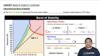
Intepreting the Band of Stability
Doping in Semiconductors
Doping involves adding impurities to a semiconductor to change its electrical properties. N-type doping introduces extra electrons, while P-type doping creates 'holes' or positive charge carriers. This process modifies the band structure, affecting the position and size of the band gap, which is crucial for tailoring the semiconductor's performance in electronic devices.
Video consigliato:
Percorso guidato
Metalloid Properties
Energy Bands
Energy bands in solids arise from the overlap of atomic orbitals, leading to the formation of filled and empty molecular orbitals. The filled band corresponds to the valence band, while the empty band is the conduction band. The arrangement and separation of these bands, including the band gap, dictate the material's electrical and optical properties, influencing its behavior in applications like transistors and diodes.
Video consigliato:
Percorso guidato
Intepreting the Band of Stability
Pratica correlata
Domanda del libro di testo
386
views
Domanda del libro di testo
The accompanying image shows photoluminescence from four different samples of CdTe nanocrystals, each embedded in a polymer matrix. The photoluminescence occurs because the samples are being irradiated by a UV light source. The nanocrystals in each vial have different average sizes. The sizes are 4.0, 3.5, 3.2, and 2.8 nm. (a) Which vial contains the 4.0-nm nanocrystals?
268
views
Domanda del libro di testo
Shown here are cartoons of two different polymers. Which one would have the higher melting point?
273
views
Domanda del libro di testo
Which of these molecular fragments would you expect to be more likely to give rise to electrical conductivity? Explain your reasoning. (a)
(b)
378
views
Domanda del libro di testo
Which arrangement of cations (yellow) and anions (blue) in a lattice is the more stable? Explain your reasoning. (a)
(b)
392
views