 Back
BackStructure and Properties of Solids: Crystal Lattices, Bonding, and Electronic Properties
Study Guide - Smart Notes
 Tailored notes based on your materials, expanded with key definitions, examples, and context.
Structure of Solids
Condensed Matter and Atomic Arrangement
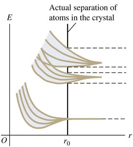
Condensed matter refers to solids and liquids, where atoms or molecules are closely packed due to strong interactions, resulting in a definite volume. In solids, atoms are separated by distances on the order of 0.1 to 0.5 nm. The arrangement of atoms determines whether a material is crystalline or amorphous.
Crystalline solids: Atoms are arranged in a long-range, repeating order (e.g., ice, copper).
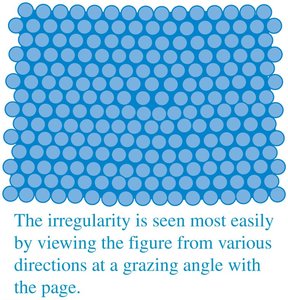
Amorphous solids: Lack long-range order but may have short-range order (e.g., glass).
Diffraction experiments (using x-rays, electrons, or neutrons) are essential for determining crystal structures, as these probes have wavelengths comparable to atomic spacings.
Crystal Lattices and Structures
Basic Lattice Types and the Basis
A crystal lattice is a repeating pattern of points in space. The basis is the atom or group of atoms associated with each lattice point. The combination of lattice and basis fully describes a crystal structure.
There are 14 unique three-dimensional lattice types (Bravais lattices).
A perfect single crystal extends this pattern uninterrupted throughout space.
Common Crystal Structures
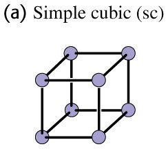
Simple Cubic (sc): Each corner of the cube is occupied by an atom. Rare in nature due to low packing efficiency.
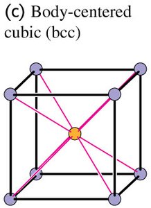
Body-Centered Cubic (bcc): Atoms at each corner and one at the center of the cube. Each atom has 8 nearest neighbors. Common in alkali metals (e.g., Na, Li, Cs, Rb).
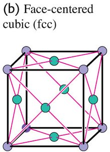
Face-Centered Cubic (fcc): Atoms at each corner and at the center of each face. Each atom has 12 nearest neighbors. Found in Al, Ca, Cu, Ag, Au.
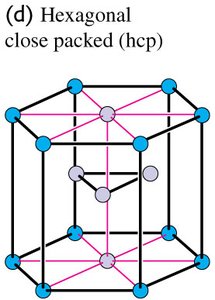
Hexagonal Close-Packed (hcp): Atoms are packed in a hexagonal arrangement, maximizing packing efficiency.
Examples of Crystal Structures
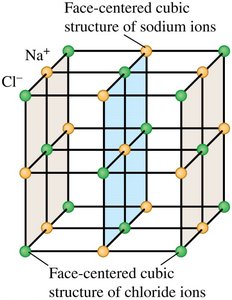
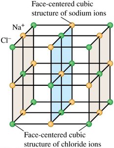
NaCl (Sodium Chloride): Appears simple cubic but is actually two interpenetrating fcc lattices (one for Na+, one for Cl–).
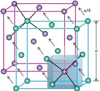
Diamond Structure: Found in carbon (diamond), silicon, germanium, and grey tin. It is an fcc lattice with a two-atom basis, where the second atom is displaced by (1/4, 1/4, 1/4) of the cube edge.
Zinc Sulphide (ZnS) and Gallium Arsenide (GaAs): Similar to diamond but with two different atoms in the basis.
Bonding in Solids
Ionic, Covalent, and Metallic Crystals
Ionic Crystals: Held together by electrostatic (Coulomb) forces between oppositely charged ions (e.g., NaCl). The arrangement depends on ion sizes and results in a stable, low-energy structure.
Covalent Crystals: Atoms share electrons in directional bonds (e.g., diamond, silicon, germanium). Each atom forms bonds with four neighbors in a tetrahedral arrangement.
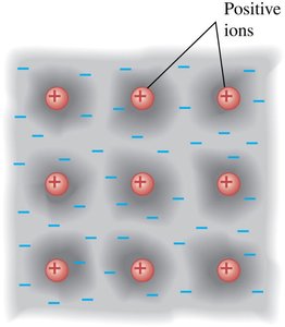
Metallic Crystals: Electrons are delocalized and shared among many atoms, forming a 'sea of electrons' that gives rise to high electrical and thermal conductivity. The structure is determined by close packing (fcc and hcp are common).

Real Crystals and Defects
Imperfections in Crystals
Real crystals are not perfect. They contain various types of defects that influence their properties:
Point Defects: Vacancies (missing atoms), interstitials (extra atoms), and substitutional impurities (foreign atoms replacing host atoms).
Extended Defects: Dislocations, such as edge dislocations, where planes of atoms slip relative to each other, affecting mechanical properties.
Polycrystalline Materials: Composed of many small crystals (grains) separated by grain boundaries.
Energy Bands in Solids
Formation of Energy Bands
When atoms come together to form a solid, their outer (valence) electron energy levels split and broaden into bands due to quantum mechanical interactions and the exclusion principle. The most important bands are:
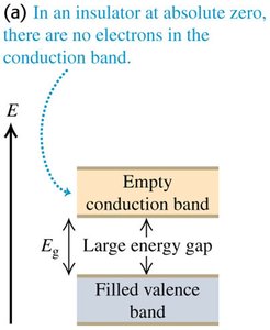
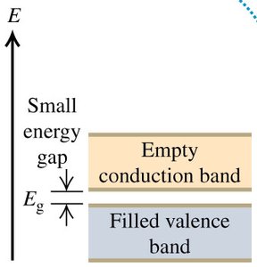
Valence Band: The highest energy band that is fully occupied by electrons at absolute zero.
Conduction Band: The next higher band, which may be partially filled or empty.
Band Gap (Eg): The energy difference between the valence and conduction bands. No electron states exist in this gap.
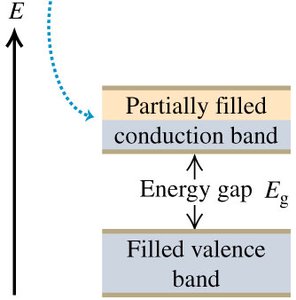
Classification by Band Structure
Type | Band Structure | Conductivity |
|---|---|---|
Insulator | Large band gap (> 5 eV); valence band full, conduction band empty | Very low |
Semiconductor | Small band gap (0.5–2 eV); valence band full at 0 K, conduction band empty | Intermediate, increases with temperature |
Conductor (Metal) | Overlapping bands or partially filled conduction band | High |
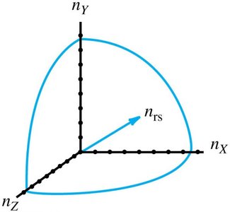
Free-Electron Model of Metals
Basic Assumptions and Density of States
The free-electron model treats conduction electrons in a metal as free particles in a three-dimensional box, ignoring interactions with ions except at the boundaries. The allowed energy levels are quantized:
The density of states g(E) gives the number of quantum states per unit energy range:
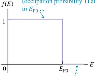
Fermi-Dirac Distribution
Electrons obey the exclusion principle and are indistinguishable, so their occupancy is described by the Fermi-Dirac distribution:
Fermi energy (EF): The highest occupied energy level at absolute zero.
At T = 0 K, all states below EF are filled, all above are empty.
Fermi Energy and Average Electron Energy
The Fermi energy for a free-electron gas is:
The average energy per electron at T = 0 K is:
Semiconductors
Intrinsic and Extrinsic Semiconductors
Semiconductors have electrical resistivity between that of conductors and insulators. Their conductivity is highly sensitive to impurities (doping).
Intrinsic semiconductor: Pure material (e.g., Si, Ge) with equal numbers of electrons and holes.
Extrinsic semiconductor: Doped with impurities to increase conductivity.
Holes and Charge Carriers
When an electron is excited from the valence band to the conduction band, it leaves behind a hole, which acts as a positive charge carrier. In intrinsic semiconductors, the number of electrons equals the number of holes.
Doping: n-type and p-type Semiconductors
n-type: Doping with Group V elements (e.g., As, P) adds extra electrons (donors) just below the conduction band, increasing electron conductivity.
p-type: Doping with Group III elements (e.g., Ga, B) creates holes (acceptors) just above the valence band, increasing hole conductivity.
Compensated Semiconductors and the Hall Effect
Semiconductors can be doped with both n- and p-type impurities, resulting in compensated materials. The Hall effect can be used to distinguish between electron and hole conduction by the sign of the Hall voltage.
Summary Table: Types of Solids and Their Properties
Type | Bonding | Structure | Examples | Conductivity |
|---|---|---|---|---|
Ionic | Ionic (Coulomb) | Crystalline (e.g., fcc) | NaCl, KBr | Low (unless molten) |
Covalent | Covalent (directional) | Diamond, tetrahedral | Diamond, Si, Ge | Low (unless doped) |
Metallic | Delocalized electrons | Close-packed (fcc, bcc, hcp) | Cu, Na, Fe | High |
Amorphous | Varied | No long-range order | Glass, plastics | Low |
