 Back
BackStructure and Properties of Solids: Crystal Lattices, Bonding, and Electronic Properties
Study Guide - Smart Notes
 Tailored notes based on your materials, expanded with key definitions, examples, and context.
Structure of Solids
Condensed Matter and Atomic Arrangement
Condensed matter refers to both solids and liquids, where atomic or molecular interactions are strong enough to give the material a definite volume. In solids, atoms are closely packed, with center-to-center separations on the order of 0.1 to 0.5 nm. The arrangement of atoms determines whether a solid is crystalline or amorphous.
Crystalline solids: Atoms are arranged in a long-range, repeating order (e.g., ice, copper).
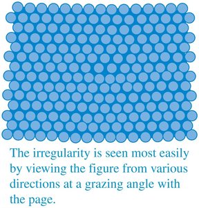
Amorphous solids: No long-range order, but short-range order exists (e.g., glass).
Crystal Structure and Lattices
The crystal structure is defined by a repeating pattern of atomic positions. A crystal lattice is a mathematical array of points in space, and a basis is the atom or group of atoms associated with each lattice point. There are 14 unique three-dimensional lattice types (Bravais lattices).
Unit cell: The smallest repeating unit in a crystal lattice.
Single crystal: A perfect, uninterrupted lattice throughout the material.
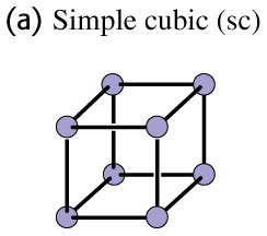
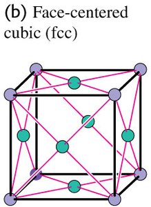
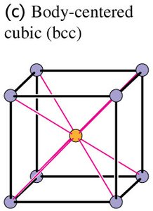
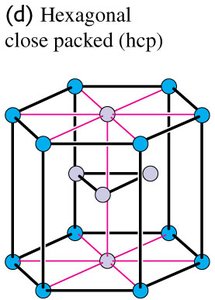
Common Crystal Structures
Several types of crystal structures are common in metals and ionic solids:
Simple Cubic (sc): Each atom has 6 nearest neighbors.
Body-Centered Cubic (bcc): Each atom has 8 nearest neighbors. Common in alkali metals (e.g., Na, Li, Cs, Rb).
Face-Centered Cubic (fcc): Each atom has 12 nearest neighbors. Found in Al, Ca, Cu, Ag, Au.
Hexagonal Close-Packed (hcp): Also features 12 nearest neighbors, but with a different stacking sequence than fcc.
Crystal Structures in Ionic and Covalent Solids
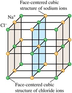
NaCl Structure: Sodium and chlorine ions each form an fcc lattice, resulting in two interpenetrating fcc lattices.
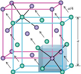
Diamond Structure: Carbon atoms (and Si, Ge, grey tin) form an fcc lattice with a basis of two atoms, one displaced by (1/4, 1/4, 1/4) of the unit cell.
Zinc Sulphide (ZnS) Structure: Similar to diamond, but with two different atoms (Zn and S) at the tetrahedral sites.
Bonding in Solids
Ionic, Covalent, and Metallic Bonds
Ionic Crystals: Held together by electrostatic (Coulomb) forces between oppositely charged ions (e.g., NaCl). The arrangement depends on the relative sizes of the ions.
Covalent Crystals: Atoms share electrons in directional bonds (e.g., diamond, silicon, germanium). Each atom forms bonds with four neighbors in a tetrahedral arrangement.
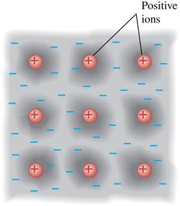
Metallic Crystals: Electrons are delocalized and shared among many atoms, forming a 'sea of electrons' that gives rise to high electrical and thermal conductivity. The structure is determined by close packing (fcc and hcp are common).
Imperfections in Real Crystals
Types of Defects
Point Defects: Vacancies (missing atoms), interstitials (extra atoms in non-lattice sites), and substitutional impurities (foreign atoms replacing host atoms).
Extended Defects: Dislocations, such as edge dislocations, where planes of atoms slip relative to each other. These defects strongly influence mechanical properties.
Polycrystalline Materials: Composed of many small single crystals (grains) joined at grain boundaries.
Energy Bands in Solids
Formation of Energy Bands
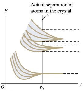
When atoms come together to form a solid, their outer (valence) electron energy levels split and broaden into bands due to quantum mechanical interactions and the Pauli exclusion principle. The resulting structure consists of:
Valence Band: The highest range of electron energies where electrons are normally present.
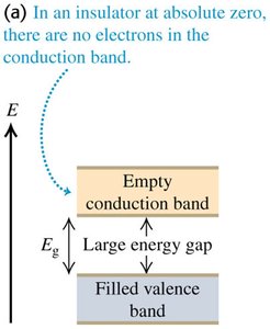
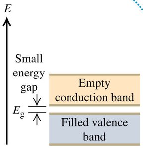
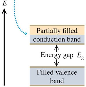
Conduction Band: The next higher range of energies, typically empty at absolute zero in insulators and semiconductors.
Band Gap (Eg): The energy difference between the valence and conduction bands. No electron states exist in this gap.

Classification by Band Structure
Insulators: Large band gap (> 5 eV); valence band full, conduction band empty at room temperature. Electrons cannot easily move to the conduction band.
Semiconductors: Moderate band gap (0.5 – 2 eV); at higher temperatures, some electrons can thermally excite into the conduction band, increasing conductivity.
Conductors (Metals): Valence and conduction bands overlap or the conduction band is partially filled, allowing electrons to move freely even at low temperatures.
Free-Electron Model of Metals
Basic Assumptions and Energy States
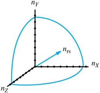
The free-electron model treats conduction electrons in a metal as free particles in a three-dimensional box, ignoring the periodic potential of the lattice except at the boundaries. The allowed energy levels are given by:
Density of States (g(E)): The number of quantum states per unit energy range is
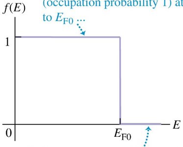
Fermi-Dirac Distribution
Electrons in solids obey the Pauli exclusion principle and are indistinguishable, so their occupancy is described by the Fermi-Dirac distribution:
Fermi Energy (EF): The highest occupied energy level at absolute zero temperature.
At T = 0 K, all states below EF are filled, and all above are empty.
Average Electron Energy
At absolute zero, the average energy per electron is
Semiconductors and Doping
Intrinsic and Extrinsic Semiconductors
Intrinsic Semiconductor: Pure material (e.g., Si, Ge) where the number of electrons in the conduction band equals the number of holes in the valence band.
Extrinsic Semiconductor: Doped with impurities to increase conductivity.
n-type Doping
Group V elements (e.g., As, P) add extra electrons (donors) just below the conduction band, increasing electron concentration.
p-type Doping
Group III elements (e.g., Ga, B) create holes (acceptors) just above the valence band, increasing hole concentration.
Holes as Charge Carriers
A hole is the absence of an electron in the valence band, behaving as a positively charged particle. In intrinsic semiconductors, electrons and holes are present in equal numbers and move in opposite directions under an electric field.
Temperature Dependence and Band Gap
The probability of electrons occupying states in the conduction band increases rapidly with temperature, especially for small band gaps.
For a band gap , the probability of occupation at the bottom of the conduction band is (assuming Fermi level in the middle of the gap).
Summary Table: Types of Solids and Their Properties
Type | Band Structure | Conductivity | Example |
|---|---|---|---|
Insulator | Large band gap (> 5 eV) | Very low | Diamond |
Semiconductor | Moderate band gap (0.5–2 eV) | Intermediate, increases with T | Silicon, Germanium |
Conductor | Overlapping bands or partially filled conduction band | High | Copper, Sodium |
Key Equations
Energy levels in a 3D box:
Density of states:
Fermi-Dirac distribution:
Average energy at T = 0:
Example: Fermi Energy in Copper
Given electron concentration
Fermi energy:
For copper,
Conclusion
The structure and bonding of solids determine their mechanical, thermal, and electrical properties. Understanding crystal lattices, energy bands, and the effects of impurities is essential for explaining the behavior of metals, insulators, and semiconductors in condensed matter physics.
